
Next-gen Electromagnetic Simulation Tool
Cloud-based, hardware-accelerated FDTD through the browser or python API
Free Sign UpProud to be a partner of leading foundries to simulate existing and develop new PDKs
Advantages of Tidy3D
Tidy3D is an electromagnetic simulation tool built on a breakthrough in computing architecture, providing scalable, accurate simulations at unprecedented speeds.
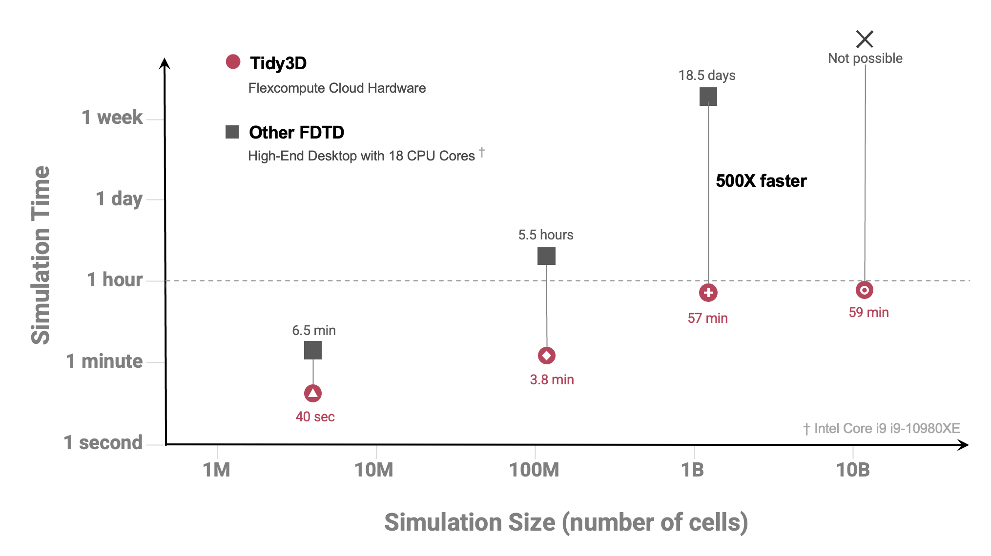
10-500x faster than workstations
100-1000x larger problem size than workstations
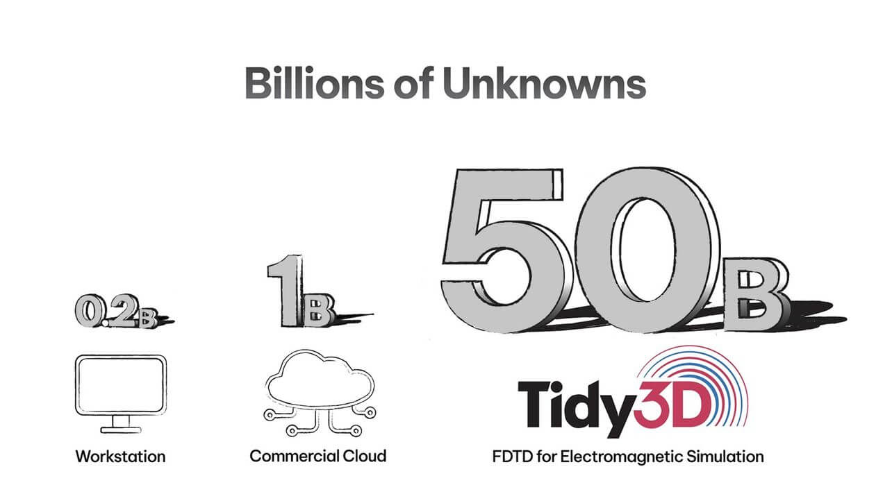
Tens to hundreds of concurrent jobs without additional licenses or computers
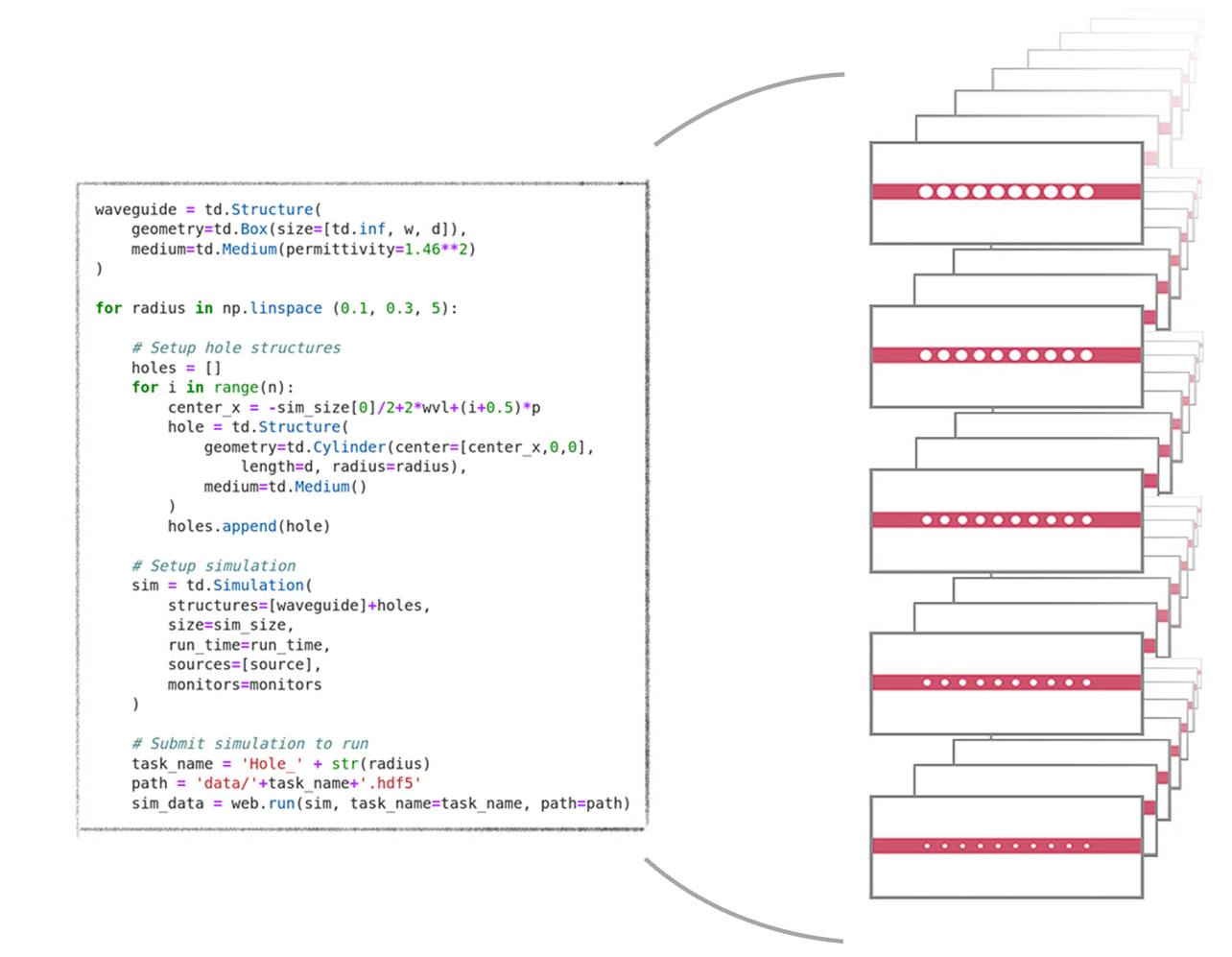
Supports both Python and Web clients. User-friendly and easily learned from scratch.


Delve into the extensive library of learning materials. Supported by our world-class solver developers and engineers.

Feature Highlight
Case Study
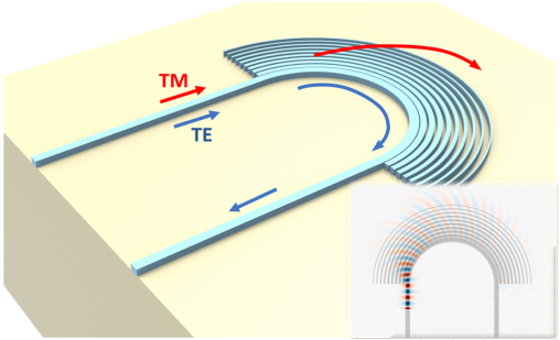
Simulating entire photonic integrated circuits without compromise
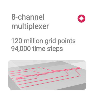
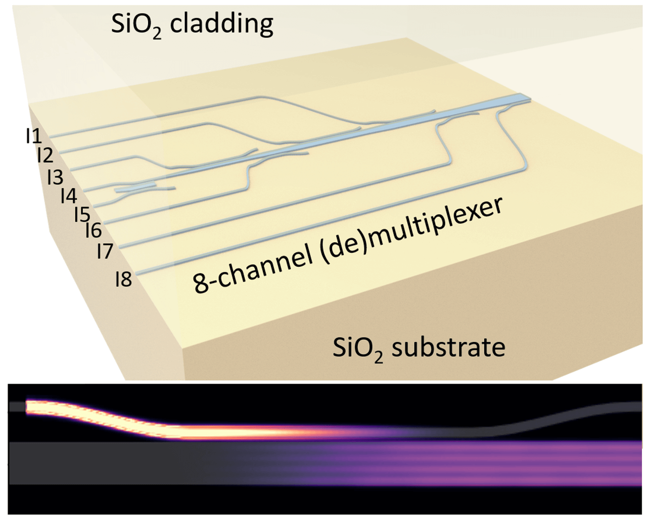
Photonic integrated circuits (PICs) can span a huge area on chip, making them hard to simulate without breaking into individual components. With Tidy3D, we are able to reliably handle entire PICs in minutes. As an example, we demonstrate the simulation of an entire 8-channel de-multiplexer based on asymmetric directional couplers.
Large PIC example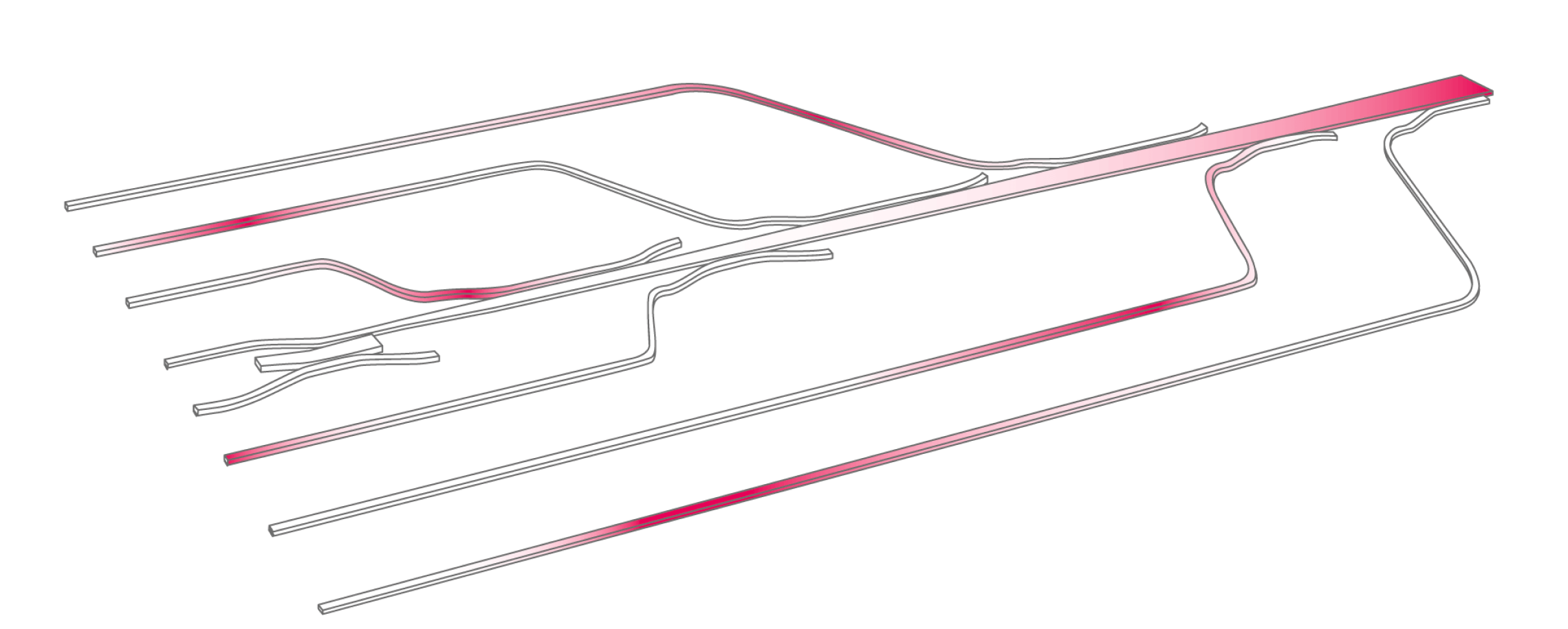
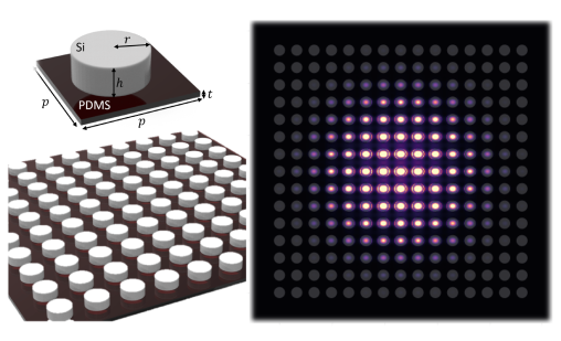
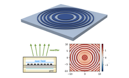
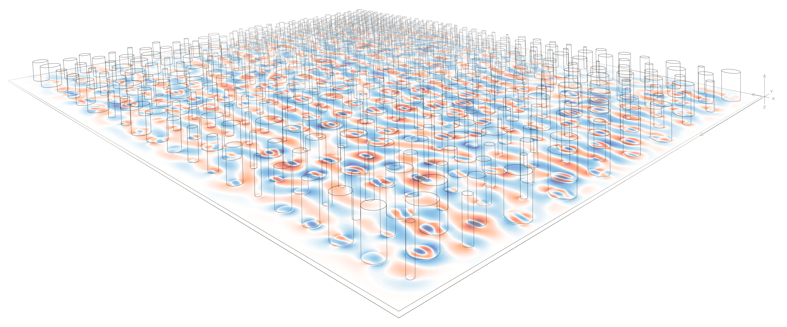
Large Area Metalens
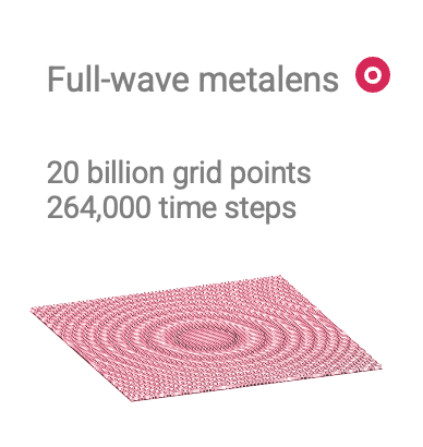
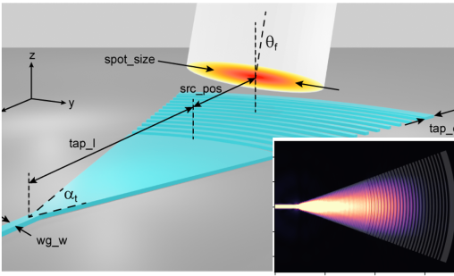
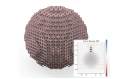
We recently simulated a large scale metalens. The device had a diameter of 100 wavelengths and required 2.7B grid cells.
This problem was too large to solve with convenential FDTD solvers, even using distributed computing. With Tidy3D, we simulated the whole device in less than 300 seconds.

Example Library
Application Areas
Customer Success

Tidy3D allows Ayar Labs to substantially shorten the design cycle of photonic circuits. Excellent agreement between simulation and actual device performance gives the R&D team the confidence to iterate their design entirely on the computer, which substantially improves product performance and reduces the time to market.
Trusted By Leading Research Institutions


